SWP scheme for short-range communication and implementation method in SIM card
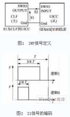
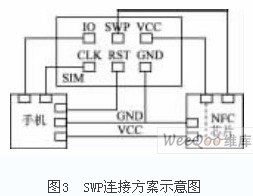
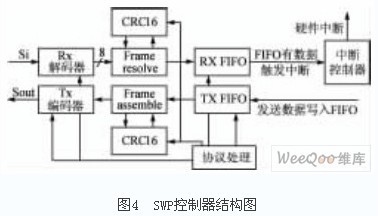
introduction In recent years, mobile phones are no longer a simple communication tool. It has become a portable entertainment tool. It is expected to develop into a reliable payment tool in the future, and it is convenient and quick to complete payment through mobile phones in the fields of consumption, shopping, transportation and the like. Based on the new demand of mobile phones, mobile payment came into being, and gradually became a hot issue for mobile operators, mobile phone manufacturers and SIM card manufacturers. There are many solutions for mobile payment, among which the dual interface SIM card solution and the Near Field Communication (NFC) solution are more feasible. The dual-interface SIM card solution has been available, and the short-range communication solution is in the development stage. The dual interface SIM card solution performs contactless communication by adding a contactless IC card interface to the SIM card. The antenna is connected to the two interfaces C4 and C8 that are not used by the SIM card. The dual-interface SIM card adds the functionality of a contactless IC card to the phone, but does not implement a reader and peer-to-peer communication. NFC is an ultra-short-range wireless communication technology proposed by NXP and Sony, which enables intuitive, convenient, and secure communication between two NFC-compatible devices. The main application of NFC is mobile micropayment, and it can also be applied to areas such as access control and public transportation. Compared with the dual interface SIM card solution, the advantages of the NFC solution are reflected in the following aspects: 1NFC solution can achieve more applications; 2 The connection between the NFC chip and the SIM card uses the C6 (SWP) contact, which does not affect the high speed air data download of the SIM card; The 3NFC solution is a complete solution that provides reliable, secure and convenient communication. The 4NFC solution is fully compatible with existing readers and does not require any changes to the reader. In summary, NFC is the most feasible solution for mobile contactless payment services, while SWP connection is part of NFC technology. 1 Overview of Near Field Communication Short-range communication is a short-range non-contact type that operates in the 13.56 MHz band and has a transmission distance of less than 10 cm. The transmission speed can now reach 106 kbps, 212 kbps, and 424 kbps, and the ideal rate can reach about 1 Mbps. NFC uses the same frequency as the current popular contactless smart card, and is compatible with ISO14443 A/B-based inductive contactless communication, as well as PHILIPS' MIFARE technology and Sony's FeliCa technology. 1.1 Principle of short-range communication According to the ISO18092 standard, short-range communication can work in active mode and passive mode. Before communication, you can select one of the transmission rates of 106 kbps, 212 kbps, and 424 kbps, and you can switch between the three. 1.1.1 Passive mode communication principle In passive mode, the communication principle of short-range communication is the same as that of RFID, which relies on the principle of electromagnetic induction coupling to complete communication. NFC phones have an NFC chip with an antenna built in to receive and transmit wireless data. When NFC works in passive mode, the reader initiates NFC communication, called an NFC originating device (master device), which provides a radio frequency domain throughout the communication process. The NFC originating device selects one type of transmission data at three rates, and the ISO 18092 standard specifies the modulation and coding techniques used for each transmission rate. The NFC target device (slave device) does not have to generate the radio frequency domain, but uses load modulation technology to transmit data back to the initiating device at the same speed. This communication mechanism is compatible with ISO14443 A/B, Mifare and FeliCa based contactless smart cards, so in passive mode, NFC originating devices can use the same connection and initialization process to detect contactless smart cards or NFC target devices, and Establish contact [1]. As far as the near-field communication application is concerned, its application modes are divided into three types: label mode, reader mode, and point-to-point mode. The tag mode, that is, the NFC chip is used as a passive device, and functions as a transponder. In order to ensure the security of the data, after the replacement of the mobile phone, the key information of the mobile payment needs to be saved in the SIM card. Communication devices include readers, NFC chips, and SIM cards. At this time, the NFC chip provides a radio frequency interface and is responsible for forwarding radio frequency data to the SIM card. For the SIM card, there is no need to add a contactless interface like a dual interface SIM card, and a connection to the NFC chip is implemented using the SWP interface. In tag mode, the NFC chip is similar to a bridge, forwarding data between the reader and the SIM card. The NFC chip is a chip embedded in a mobile phone and is powered by the power system of the mobile phone. In order to ensure the normal operation of mobile payment when the mobile phone is out of power, the tag mode needs to support passive work, and its working principle is based on electromagnetic induction. The antenna coil of the reader produces a high frequency, strong electromagnetic field that passes through the cross section of the coil and the space around the coil. A portion of the magnetic field lines that emit the magnetic field pass through the antenna coil [2] of the transponder at a distance from the reader coil. A voltage is generated on the antenna coil by induction, rectified and supplied as a power source to the NFC chip and the SIM card. 1.1.2 Principle of Active Mode Communication In the active mode, when the NFC initiator sends data to the target device, it must generate its own RF field. When the read NFC device sends a response to the initiator, it also generates its own RF field. Both the initiating device and the target device must generate their own RF field, which is the standard mode for peer-to-peer network communication and can achieve very fast connection settings [1]. Mobile devices work primarily in passive mode, which dramatically reduces power consumption and extends battery life. Active mode is mainly for point-to-point mode, used for data exchange between notebooks, mobile phones, and digital cameras. 1.2 The relationship between short-range communication and RFID NFC is an RFID-based wireless communication technology that operates in the 13.56 MHz band. In the tag mode, NFC uses the communication principle of RFID, which is based on the principle of electromagnetic induction coupling of wireless frequencies. However, NFC technology is a new technology for wireless communication. It is different from RFID: NFC technology adds point-to-point communication function, and can quickly establish P2P (peer-to-peer) wireless communication between Bluetooth devices. NFC devices look for each other and establish communication connections. Both devices of the P2P communication are peer-to-peer, and the devices of the RFID communication are master-slave relationships. 2 SWP standard and connection scheme 2.1 SWP Standard [3] The SWP connection scheme is based on the ETSI (European Telecommunications Standards Institute) SWP standard, which specifies the communication interface between the SIM card and the NFC chip. SWP (Single Line Protocol) is a full-duplex communication on a single line, that is, the signals in the two directions S1 and S2, as shown in Figure 1. The two sides of the communication are UICC (Universal Integrated Circuit Card) and CLF (Contactless Front-end). S1 is a voltage signal, the SIM card detects the high and low levels of the S1 signal through the voltmeter, and adopts level-width modulation; the S2 signal is a current signal, and adopts a load modulation method. The S2 signal must be active when the S1 signal is high. When the S1 signal is high, it turns on a triode inside it, and the S2 signal can be transmitted. The S1 signal and the S2 signal are superimposed to achieve full-duplex communication on a single line [4]. The encoding of the S1 signal is shown in Figure 2. Logic 1 is high for 3/4 cycles (3/4T) and logic 0 is high for 1/4 cycle (1/4T). The S2 signal is active when the S1 signal is high, and can be switched from low to high when the S1 signal is low. SWP has three transmission rates: 212 kbps, 424 kbps, and 848 kbps. After expanding the data bits, the transmission rate can reach 1 696 kbps. The SWP protocol is a protocol for the physical layer and the data link layer. The physical layer is responsible for the activation, maintenance, and deactivation of the physical link between the UICC and the CLF. The SWP protocol requires the operating voltage of the UICC to be 1.8 to 3.3 V. Similar to the OSI protocol, the data link layer is divided into a MAC (Media Access Control) layer and a link control layer. A bit-filling framing method is employed at the MAC layer. The link control layer includes three types of frame protocols: the ACT protocol, the SHDLC protocol, and the CLT (Contactless Channel) protocol. In the design of the SWP interface, the first two protocols are used. The ACT protocol is an interface activation protocol used to activate the SWP interface. When there is no RF field, the SWP interface is deactivated. In the tag mode, after the external RF field is sensed, the NFC chip is activated. After receiving the high-level signal of the NFC chip, the UICC uses the ACT frame to establish a physical link connection. The SHDLC protocol is a simple version of the advanced data link control specification developed by ISO and is a bit-oriented synchronous link. The protocol is mainly used to transmit interactive data information, and the information frame carries the packet data of the upper layer HCP (Host Control Protocol). In addition, the SHDLC protocol also has functions such as flow control management, error checking, and data retransmission after error. In order to ensure the correct transmission and reception of data, it is compatible with the communication capability of the NFC chip and the UICC at different rates. Before using the SHDLC protocol for communication, the data link must first be established, and the size of the sliding window is negotiated by both parties. 2.2 SWP connection scheme In this paper, the CLF is embedded inside the mobile phone, and the UICC uses the SIM card, and the mobile phone communicates with the NFC chip through the SIM card. There are many connection schemes between NFC chip and SIM card. This paper proposes a SWP (single line protocol) scheme based on C6 pin. The SWP protocol connects the mobile phone NFC chip with the SIM card and specifies the communication interface between the two. Figure 3 is a schematic diagram of a SWP connection scheme. This solution uses three pins of the SIM card to connect to the NFC chip: C1 (VCC), C5 (GND), and C6 (SWP). Among them, the SWP pin achieves full-duplex communication based on voltage and load modulation principles on a single line. The SIM card supports two interfaces, ISO7816 and SWP. In the large-capacity card project, the high-speed download interface is also supported, which is realized by the reserved C4 and C8 interfaces. The SIM card supporting SWP must support two protocol stacks - ISO7816 and SWP protocol stack. This requires the COS (on-chip operating system) of the SIM card to be a multi-tasking system. The SIM card needs to manage these two protocol stacks separately. After the SWP solution is added to the SIM card system, it cannot affect the ISO7816 interface. For example, the SIM card has 8 pins, and the RST pin is used to reset the ISO7816 interface of the SIM card. After the SWP scheme is added to the SIM card, the Reset signal of the RST pin has no effect on the SWP interface, and the SWP interface is reset by the SWP pin. . 3 SWP connection scheme design in SIM card 3.1 System Structure The high-capacity SIM card is a smart card that supports mass storage, high-speed transmission, and new applications. The high-capacity SIM card project we developed is based on the ARM Secure Core SC100 core and uses the AHB (High Performance Bus) + APB (Advanced Peripheral Bus) bus architecture. The AHB bus provides high-speed data transfer, which connects the SIM card internal memory to the high-speed external interface (USB interface). The APB bus is connected to the AHB bus through a bridge, and the low-speed interface of the SIM card (SWP interface, ISO7816 interface) is attached to the peripheral bus. 3.2 Hardware Design The SWP hardware design is based on the SWP standard, TS 102 613 developed by ETSI (European Telecommunications Standards Institute). The SWP controller and the SWP interface together form the hardware device of the SWP solution. The SWP controller handles the physical layer and data link layer logic. 4 is a structural diagram of an internal SWP controller of a SIM card when hardware implements data link layer logic. 3.2.1 Receive data design During communication between the SIM card and the NFC chip, the SWP controller switches between three states of activation, suspend, and deactivation. When data is exchanged, it is active. The Rx decoder continuously detects the Si signal and parses the unit data from the NFC chip into a byte output. Frame. resolve analyzes each byte of data received, if it is 7E (frame header), continues to receive data until it receives 7F (end of frame), indicating that SWPC received a complete frame of data. Frame. resolve further parses the received data frame, first strips the frame header and the end of the frame according to the MAC protocol, and then verifies the data frame according to the generator's generator polynomial. If the data is correct, the type of the SHDLC data frame is identified and processed accordingly; if the data is incorrect, the rejected frame is sent and the other party is required to resend. For the correct information frame, the SWP controller extracts the information data (packet) of the information frame into the RX FIFO, and sets the controller's status register according to the number of bytes of the received data frame. The SWP controller initiates a hardware interrupt each time it receives a frame of data. 3.2.2 Sending data design The SWP controller sends and receives data in reverse. If the upper application has data to send, it will write the data to the TX FIFO. Once the TX FIFO detects that there is data in the FIFO, it starts the sending module to take the data out of the TX FIFO, assembles the information frame according to the SHDLC protocol of the SWP protocol, and adds the frame header, the end of the frame, and the check code. The generated MAC frame data is passed to the Tx encoder to complete the physical layer assembly of the output data, and the data is converted into a single bit level output. 3.3 Software Driven Design The SWP software design is based on the SWP standard and the HCP (Host Control Protocol) standard. The HCP standard is a standard protocol on top of the SWP protocol, defining the protocol layer above the data link layer - the HCP routing layer, the HCP message layer, and the application layer [5]. The protocol stack consisting of the underlying SWP protocol and the upper HCP protocol completes the complete protocol of the NFC chip and UICC communication. The SWP scheme is adopted in the large-capacity SIM card, and the ISO7816 protocol stack and the SWP protocol stack are implemented. The SIM card's operating system uses μC/OS. μC/OS is a compact, preemptive real-time operating system. Its core provides tasks scheduling and management, time management, task synchronization and communication, memory management and interrupt services. In software systems, the SWP software module is one of the tasks of μC/OS. The SWP task relies on a hardware interrupt driver, and the SWP task is in a state of waiting for an interrupt before it is activated. When communicating via the SWP interface, the NFC chip is activated upon detection of the presence of the RF field. The NFC chip sends the Si signal to the SIM card. After the SIM card detects the Si voltage signal, it triggers the si_act interrupt to notify the software to prepare for communication. At this point, the software sets the communication parameters and then waits for the hardware to establish a successful physical link interrupt. If the init_sync interrupt is received, the software starts to set the sliding window size M of the SHDLC protocol, waiting for the interrupt of the SHDLC link to be established. This interrupt has the parameter N of the sliding window with the SHDLC layer of the NFC chip. If M ≥ N, the SWP task modifies its own sliding window size to N, and then sends an acknowledgment frame, thus establishing an SHDLC link; After the SHDLC link is successfully established, the SWP task waits for the information frame to be interrupted. After receiving the information frame interrupt, the data is read from the RX FIFO according to the number of received bytes of the status register written by the hardware, and then the received data packet is parsed by the software; the data packet is delivered to the application layer through the routing layer of the HCP, and the application is applied. The layer performs corresponding processing according to the type of the message. Conclusion This paper proposes a SWP connection scheme and implements it in a large-capacity SIM card. The hardware and software design method of SWP interface has certain reference significance for the application of short-range communication technology to other mobile payment. At the same time, the realization of SWP interface in SIM card also promotes the development of SIM card technology. CD Envelope,Disk Envelope,White CD Envelopes,Skyline White CD Envelope Sun Kee Envelopes Limited , https://www.sunkeeenvelope.com